LC-3 Instructions
| Type | Quiz 3 Material |
|---|
This video saves lives:
LC3 Reference Sheet
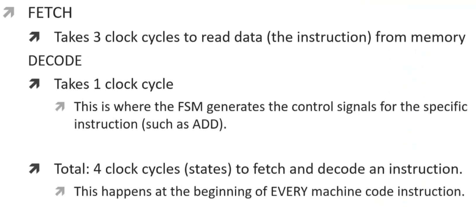
Every instruction starts with 4 phase:
Fetch
Fetch
Fetch
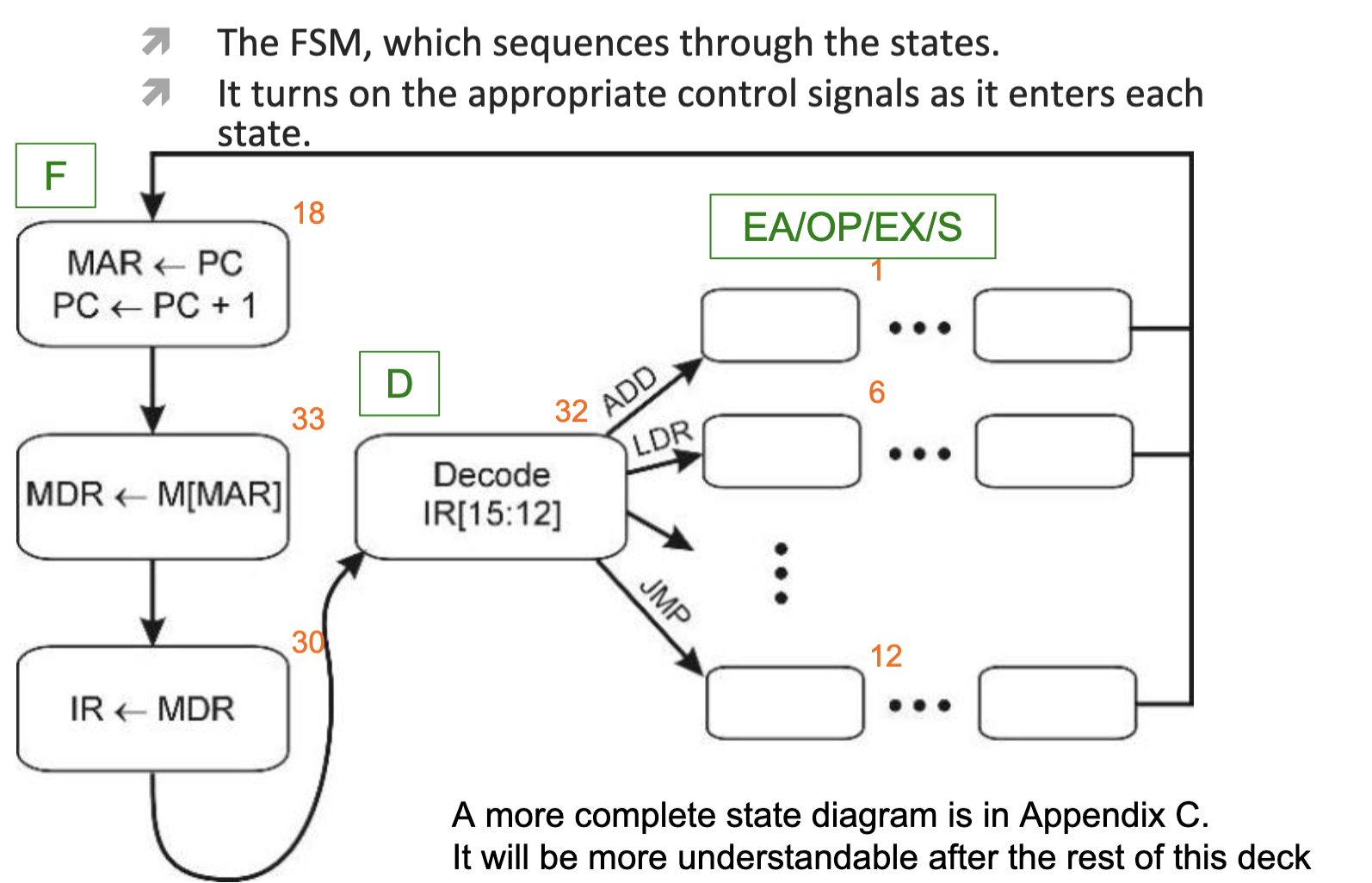
Decode —> FSM
FSM
FSM execute microcode
Confusions:
Clock Cycle
You want to maximize what happens during a single clock cycle. There are 2 main obstacles that help determine what cannot happen during a single clock cycle.
1. A register is only updated with its new value on the rising edge of the clock. If you need to use the value of the register you just set, then you must wait till the next clock cycle. An example of this would be a load instruction. If you set the value of MAR in the first clock cycle, then you must wait until the next clock cycle to read MAR. You cannot set and read from the register in the same clock cycle.
2. Only one value can be on the bus at any given time. If you need to set 2 different registers with different values, this will take 2 clock cycles since only one value can be on the bus. An example of this would be a store instruction. You need one clock cycle to set MDR and another to set MAR.
LD.CC
Any time you do an instruction that changes the value of a register in the register file, you need to set the condition codes because there is a possibility that we require the sign of that value to determine branching (BR) logic. The exception to this rule is for LEA. LEA will always load into a register a binary string that represents an address. It doesn't make sense for an address to be signed, so we do not set a condition code for it. That also means you should not complete Branching logic based on LEA! It's just an address in memory. Instead, it would make more sense to load the data at that address since that could be a more meaningful value. We have made this note in the LC-3InstructionsDetail.pdf
For the remainder of instructions that do set condition codes, since there is a possibility that they could store a meaningful number/result of math/ value (ie: not an address) into a register that means we need to set the cc's. We might not BR based on the CC each time we do one of these operations, but since that possibility does exist, we have to include setting CC in these instructions microcodes.
EDIT: please note that when we change a value in memory (ie: perform a store) we do not set condition codes. This is because memory is not a register
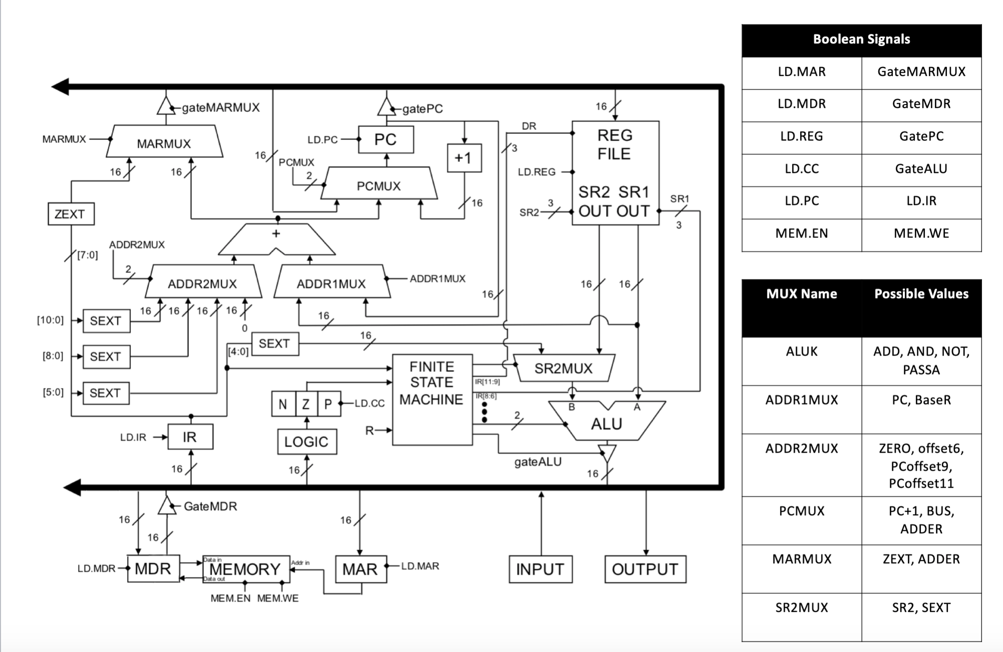
Fetch
IR <= Mem[(PC)]
Control Instructions
- Clock Cycle 1:
- PCMUX selects PC.MUX + 1
- LD.PC
- Gate.PC - allow data to flow from PC to bus
- LD.MAR - Load the data to memory
- Clock Cycle 2:
- MEM.EN/R - Memory read data
- (MDRMUX select memory - take data from memory and send to the bus)
- LD.MDR - Write data into the MDR
- Clock Cycle 3:
- Gate.MDR - Write data to the main bus
- Load.IR - Read data to the IR
- Clock Cycle 1:
OPERATE:
Add
Definitions

DR = (SR1) + (SR2)
Control Instruction
One clock cycle
- (SR1MUX select IR[8:6])
- SR2MUX selects OUT
- ALUK select add - add SR1 and SR2 - 00
- GateALU - send added data to the bus
- LD.REG - write the data to the destination register
- LD.CC
DR = (SR1) + SEXT[IR[4:0]]
Control Instruction
One clock cycle
- SR1MUX select IR[8:6] - 1
- SR2MUX selects SEXT[IR[4:0]] - Sign extended SR2
- ALUK select add - add SR1 and SR2
- GateALU - send added data to the bus - 1
- LD.CC - 1
- LD.REG - write the data to the destination register - 1
AND
Definitions

DR = (SR1).(SR2)
One clock cycle
- (SR1MUX select IR[8:6]) - 1
- SR2MUX select SR2 OUT
- ALUK select AND - 01
- Gate.ALU - 1
- LD.CC - 1
- LD.REG - 1
NOT
Definitions

DR <= (SR1’)
One clock cycle
- SR1MUX select IR[8:6] - 1
- ALUK Select NOT
- Gate.ALU - 10
- LD.CC - 1
- LD.REG - 1
LOADS:
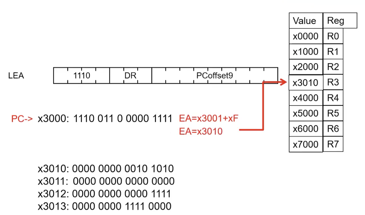
LEA(LOAD EFFECTIVE ADDRESS)
Definitions
Puts the effective address (PC+offset) itself into a register (no memory access!)

DR <= (PC) + SEXT(IR[8:0])
One clock cycle
- ADDR1MUX Select PC - 0
- ADDR2MUX Select SEXT(PCoffset9/IR[8:0]) - 10
- MARMUX select ADDER - ADD also send data to MARMUX.gate instead of PC - 1
- Gate.MARMUX - Send data to the main bus - 1
- LD.REG - Take data from bus and load to destination register - 1
Binary Encoding Example
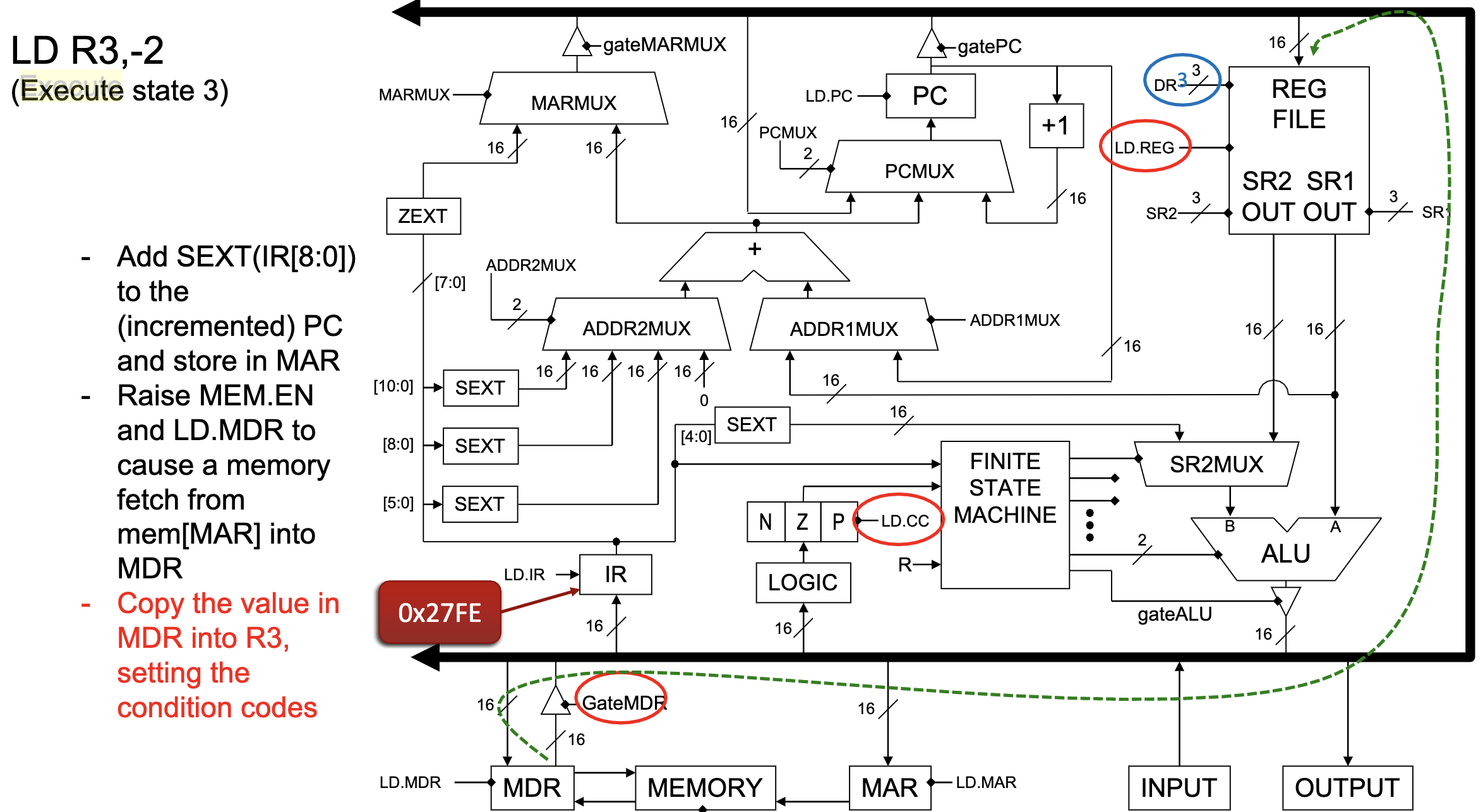
LD(LOAD)
Definitions
Puts the contents of some memory at the effective address (PC+offset) into a register

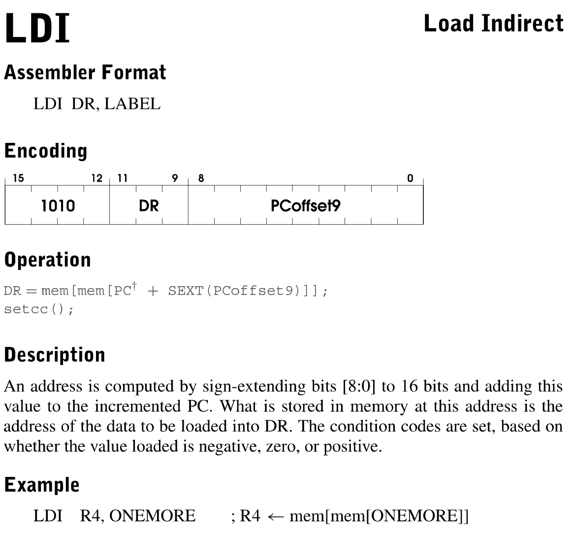
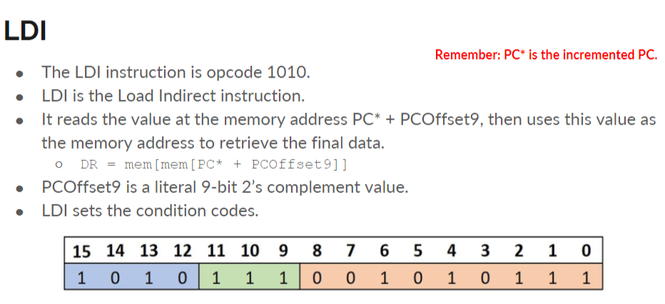
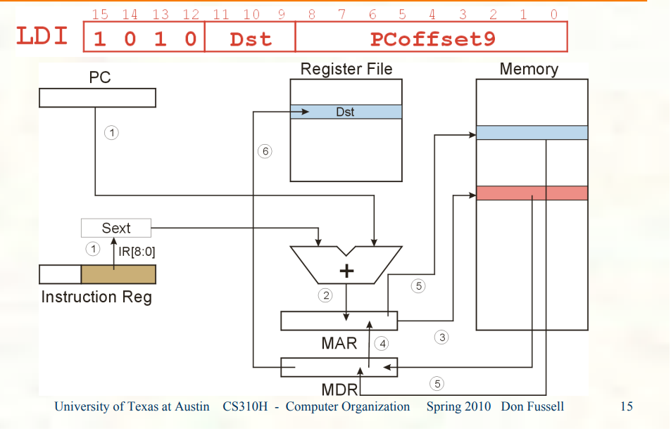
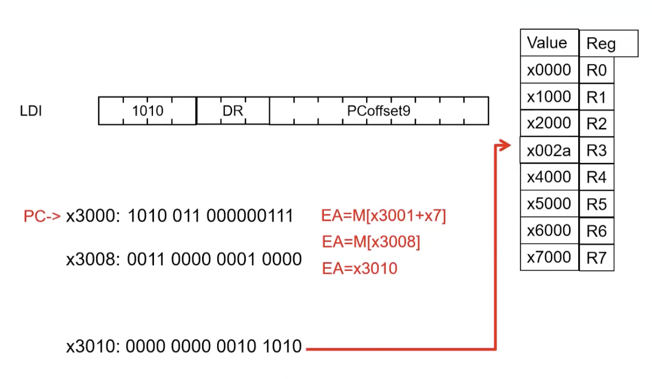
LDI(LOAD INDIRECT)
Definitions
Goes to the effective address (PC+offset) and gets a value. Treats that value as another memory address, and gets data from there, into a register (hits memory twice)
- Clock cycle 1
- ADDR1MUX Select PC - 0
- ADDR2MUX Select SEXT(PCoffset9) - 10
- MARMUX selects ADDER - 1
- Gate.MARMUX - 1
- LD.MAR - 1
- Clock Cycle 2
- MEN.EN - 1
- LD.MDR(MDRMUX select memory) - 1
- Clock Cycle
- Gate.MDR - 1
- LD.MAR - 1
- Clock Cycle 4
- MEN.EN - 1
- LD.MDR(MDRMUX select memory) - 1
- Clock Cycle 5
- Gate.MDR - 1
- LD.CC - 1
- LD.REG - 1
- Clock cycle 1
Binary Encoding Example
LDR(LOAD BASE + OFFSET)
Definitions
Puts the contents of the effective address (base register+offset) into a register.
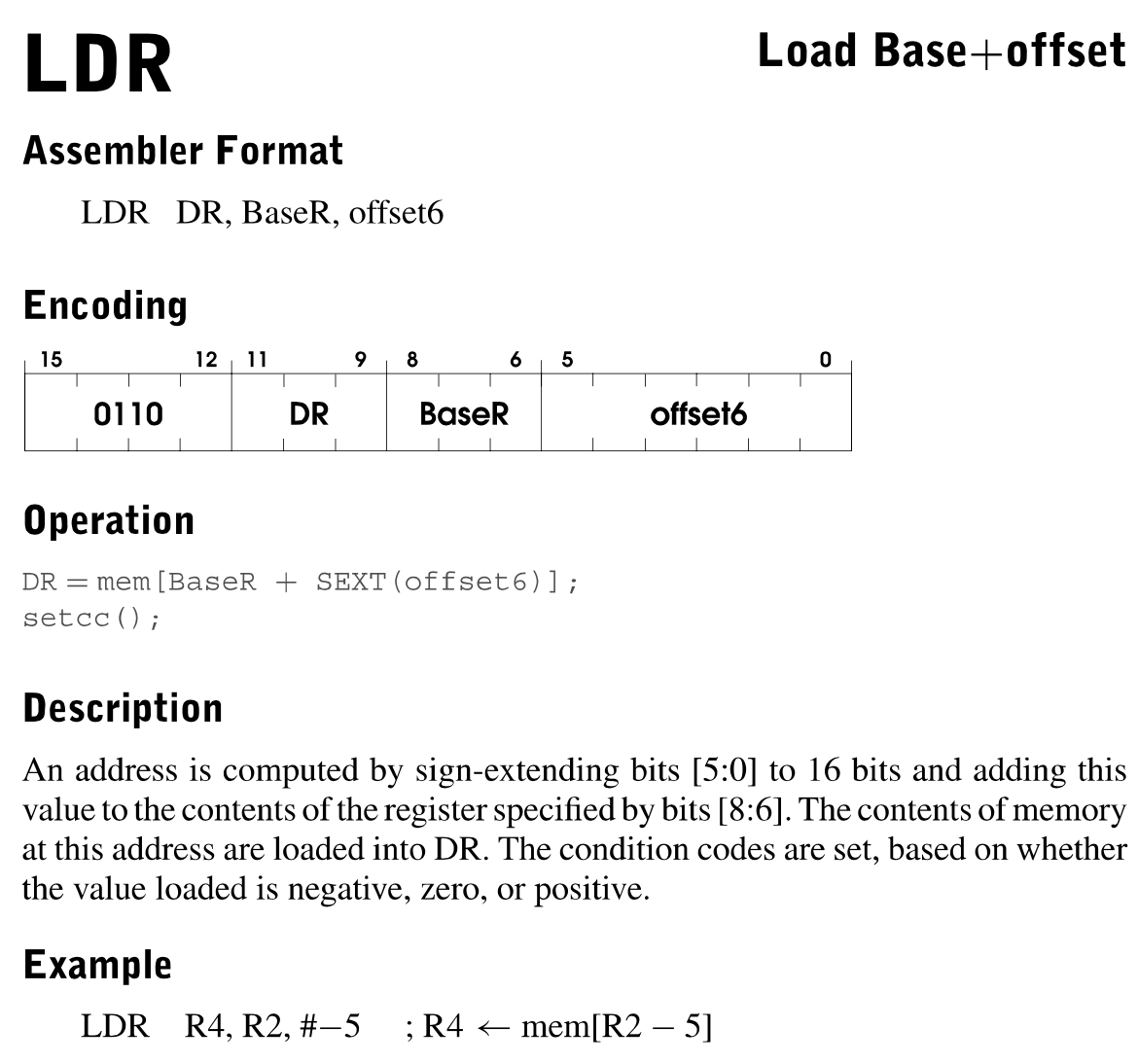
DR < = Mem[IR[8:6] + SEXT(IR[5:0])]
- Clock Cycle 1
- ADDR1MUX selects SR1OUT - 1
- ADDR2MUX selects SEXT(IR[5:0]) - 01
- MARMUX selects ADDER - 1
- Gate.MARMUX - 1
- LD.MAR - 1
- Clock Cycle 2
- MEN.EN - 1
- LD.MDR(MDR.MUX select Memory) - 1
- Clock Cycle 3
- Gate.MDR - 1
- LD.CC - 1
- LD.REG - 1
- Clock Cycle 1
STORES:
ST(STORE)
Definitions
Puts the contents of a register into memory at the effective address (PC+offset).
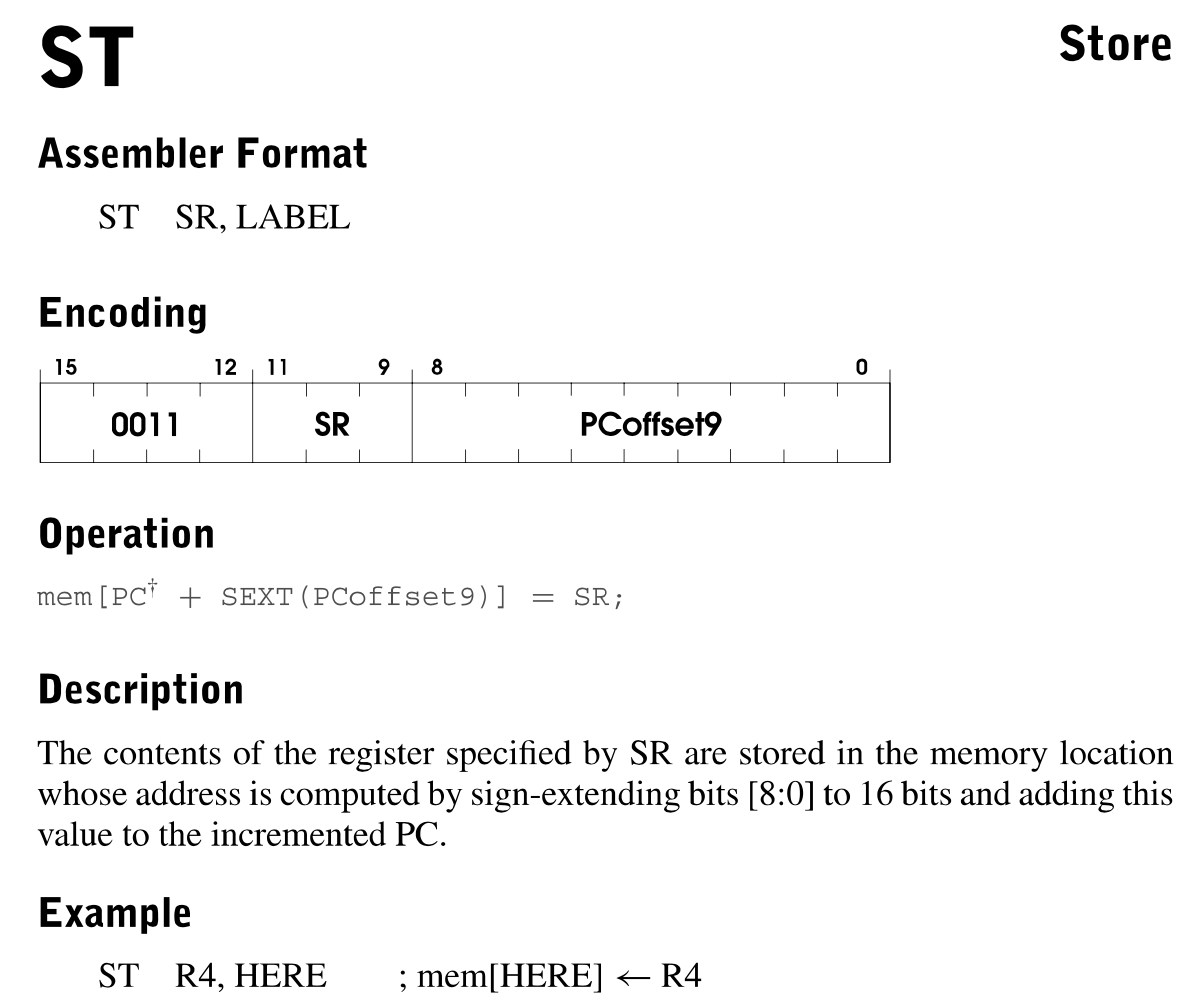
Mem[(PC) + SEXT(IR[8:0])] < = SR
- Clock Cycle 1
- ADDR1MUX select PC - 0
- ADDR2MUX select SEXT(IR[8:0]) - 10
- MARMUX select ADDER - 1
- Gate.MARMUX - 1
- LD.MAR - 1
- Clock Cycle 2
- SR1 - 0
- ALUK selects PASS - 11
- Gate.ALU —> Pass to bus and send it to MDR - 1
- LD.MDR(MDRMUX select BUS) —> Take the source register from BUS - 1
- Clock Cycle 3
- MEM.EN - 1
- R.W - 1
- Clock Cycle 1
Binary Encoding Example
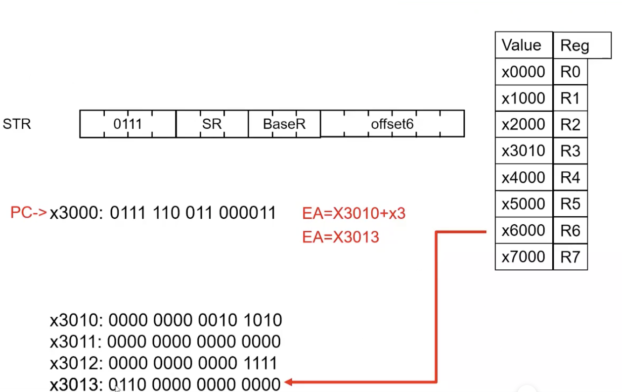
STR(STORE BASE + OFFSET)
Definitions
Puts the contents of a register into memory at the effective address (base register+offset)
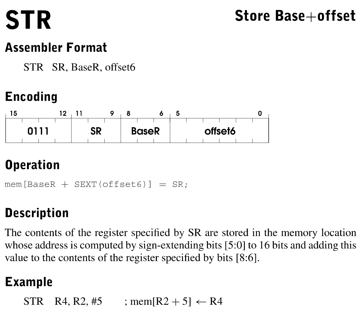
Mem[(IR[8:6]) + SEXT(offset6)] < = SR
- Clock Cycle 1
- (SR1MUX select IR(8:6))
- ADDR1MUX select BaseR - 1
- ADDR2MUX select SEXT(offset6) - 01
- MARMUX select ADDER - 1
- Gate.MARMUX - 1
- LD.MAR - 1
- Clock Cycle 2
- Gate.ALUK - 1
- ALUK select PASS - 11
- LD.MDR - 1
- Clock Cycle 3
- MEM.EN - 1
- R.W. - 1
- Clock Cycle 1
Binary Encoding Example
STI(STORE INDIRECT)
Definitions
Puts the contents of a register into a memory location whose address is stored in memory at the effective address (PC+offset). (Hits memory twice!)
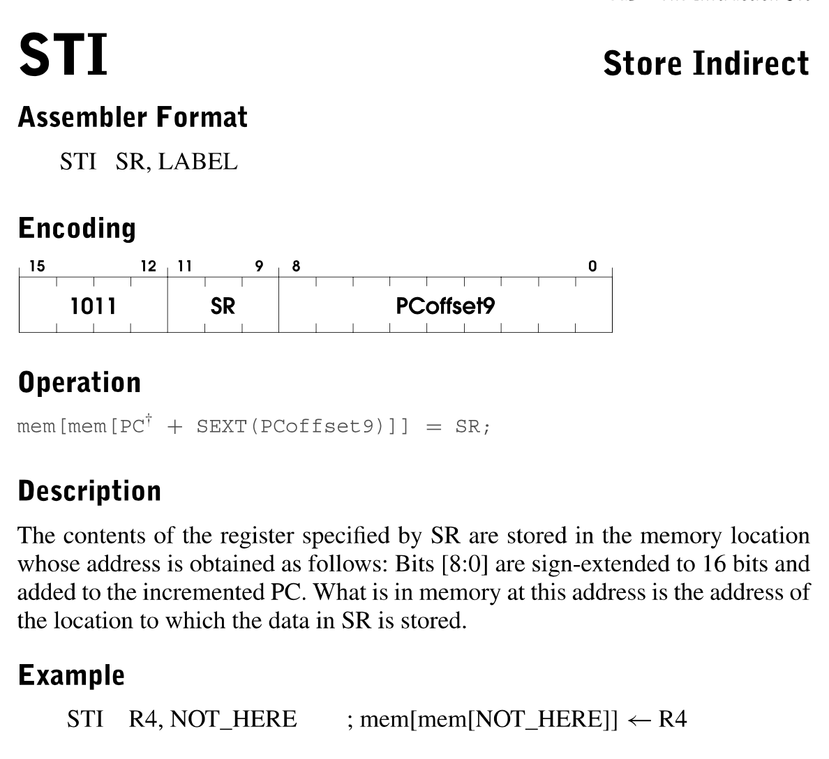
Mem[Mem[(PC) + SEXT(IR[8:0])]] < = SR
- Clock Cycle 1
- ADDR1MUX select PC - 1
- ADDR2MUX select SEXT(IR[8:0]) - 10
- MARMUX select ADDER - 1
- Gate.MARMUX - 1
- LD.MAR - 1
- Clock Cycle 2
- MEM.ER - 1
- LD.MDR (MDRMUX select Memory) - 1
- Clock Cycle 3
- GATE.MDR - 1
- LD.MAR - 1
- Clock Cycle 4
- Gate.ALUK - 1
- ALUK select PASS - 11
- LD.MDR - 1
- Clock Cycle 5
- MEM.EN - 1
- R.W. - 1
- Clock Cycle 1
CONTROL:
JMP(JUMP)
Definition
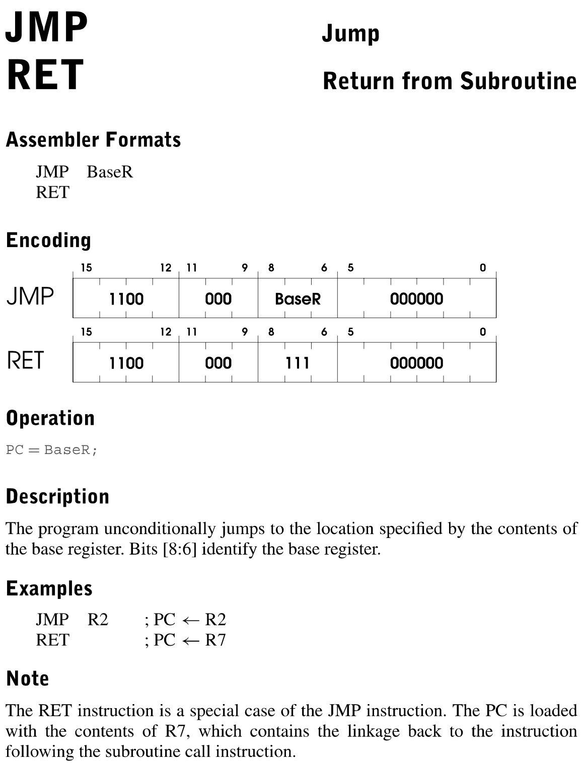
PC < = (BaseR)
- (SR1MUX select IR[8:6])
- (ADDR1MUX select SR1OUT)
- ADDR2MUX select ZERO
- PCMUX select ADDER —> Add SR1 with 0(Changes nothing) and send to PC
- LD.PC
BR(CONDITIONAL BRANCH)
Definitions
nzp are conditional branch instructions, determine whether the change the instruction flow.
During the EXECUTE phase, the processor examines the condition codes whose corresponding bits in the instruction are 1.
If any of nzp are 0, the corresponding condition codes are not examined.
If any of the condition codes that are examined are in state 1, then the PC is loaded with the address obtained in the EVALUATE ADDRESS phase
Example
PC = x4027
Example: 0000 010 011011001
Assembly: BR z x0D9
Next instruction: Instead of x4028, it would be x4028 + x0D9 = 4101
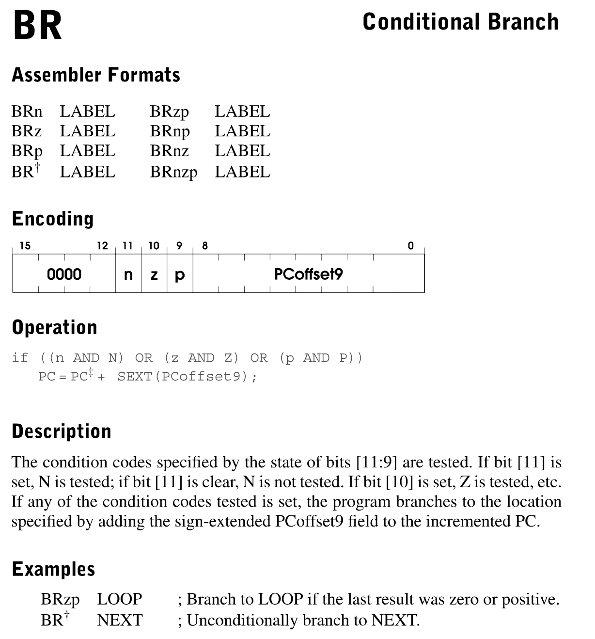
PC < = (PC) + SEXT(IR[8:0]) iif (N.n + Z.z + P.p)
- ADDR1MUX select PC
- ADDR2MUX select SEXT(IR[8:0])
- PCMUX select ADDER
- LD.PC iif (N.n + Z.z + P.p)
JSR & JSRR(JUMP TO SUBROUTINE)
Definition
If JMP is located at x4000 and baseR is x6600, the program will execute the x4000(JMP) followed by the instruction at x6600
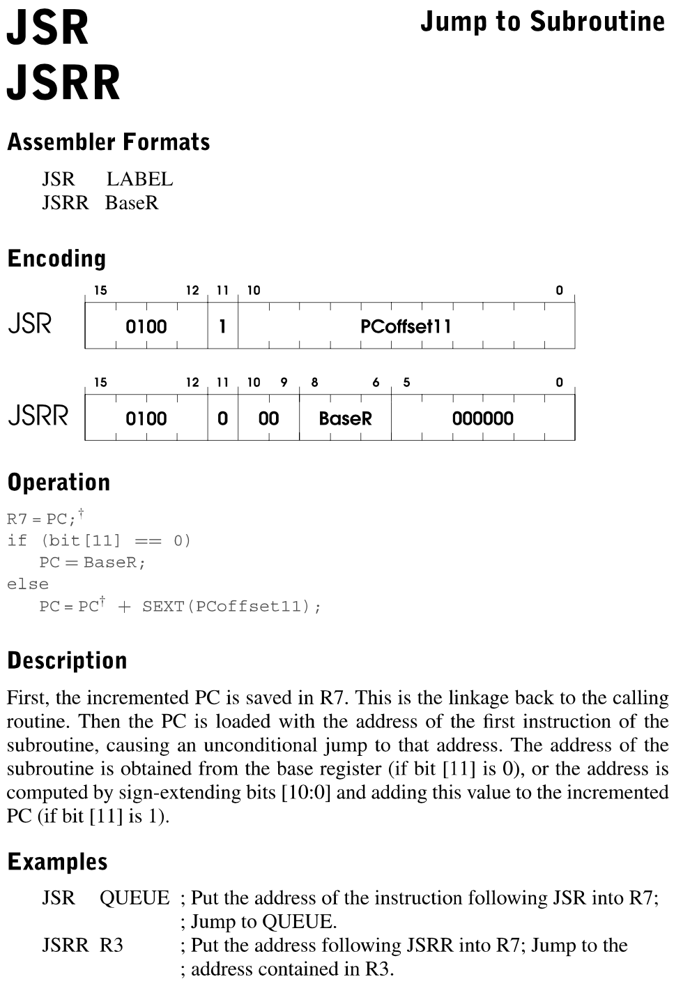
JSR
R7 < = (PC). PC < = (PC) + SEXT(IR[10:0])
- GatePC
- DRMUX select [111]
- LD.REG
- ADDR1MUX select PC
- ADDR2MUX select SEXT(IR[10:0])
- PCMUX select ADDER
- LD.PC
JSRR
R7 ≤ PC. PC < = (BaseR)
Instruction 1
- GatePC
- DRMUX select [111]
- LD.REG
TRAP
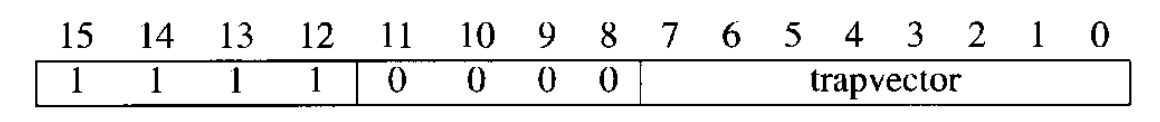
Trapvector: identifies the service call that the program wishes the operating system to perform
- Once the operating system is finished performing the service call, the program counter is set to the address of the instruction following the TRAP instruction.
- In this way, a program can, during its execution, request services from the operating system and continue processing after each such service is performed.
Servical Calls:
- Input a character from the keyboard (trapvector = x23)
- Output a character to the monitor (trapvector = x21).
- Halt the program (trapvector = x25)
